Another heavyweight personnel turmoil in the domestic chip industry! According to Observer Network, Jiao Guofang, co founder of domestic GPU Black Horse Wall Ren Technology and general manager of graphics GPU product line, has resigned, and the reason for his resignation is not yet clear.
25 years of experience, GPU leader resigns, holding 50+patents
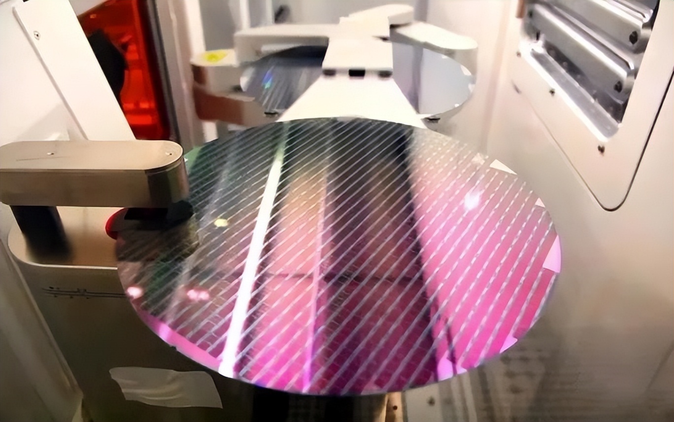
According to the official website, Bi Ren Technology was founded in 2019 and mainly develops General Purpose GPUs (GPGPUs) for use in fields such as artificial intelligence training and reasoning. Jiao Guofang, who was rumored to have resigned this time, is one of the technology giants in Bi Ren Technology. In 2021, along with the announcement of the launch of a new product line for graphics GPUs by Bi Ren Technology, it was also announced that Jiao Guofang, co founder of Bi Ren Technology, would serve as the general manager of the graphics GPU product line.
Regarding the entry of Bi Ren into the graphics processing field, Jiao Guofang has publicly stated: “Compared to the artificial intelligence market, the integration of the graphics GPU market is higher. Bi Ren Technology, with its advantages of being closer to the Chinese market and international technological strength, conducts in-depth optimization for local and emerging application scenarios
Looking up his past resume, it shows that Jiao Guofang has over 25 years of GPU product architecture and research and development experience. He has worked at Qualcomm for 11 years and, as the head of the GPU team, independently developed the 5th generation classic Qualcomm Adreno mobile GPU architecture.
It is reported that during his tenure at Qualcomm, Jiao Guofang participated in the research and development of over 50 patents as an inventor, with 100% being invention patents. The patents invented by Jiao Guofang mainly focus on professional technical fields such as graphics processing units, shaders, compilers, arithmetic logic units, buffers, multimedia processors, etc.
In addition, the patent “Multi stage Embedding of Graphic Description” jointly invented by Jiao Guofang, Wei Jian, Bi Ning, and Wu Jianwei (publication number TW201001329A) has been cited as many as 20 times by peers in the same industry. This patent was filed in 2008 and was cited by other companies’ patents until 2019.
In addition to his experience at Qualcomm, Jiao Guofang has also served as the Chief Scientist of GPU Technology in Huawei Futurewei, responsible for Huawei Hongmeng OS graphics and image processing and UI system framework.
Previous industry sources have shown that Jiao Guofang’s resignation may be mainly due to a conflict between him and Zhang Wen, the founder and CEO of Bi Ren Technology, regarding the company’s development direction and control rights.
It is reported that Zhang Wen, the founder and CEO of Bi Ren Technology, was initially a “layman” in the GPU (graphics processor) field without industry background. During the initial search for investors, Zhang Wen later told early investors, “At that time, in the big chip race, I was the only founder who didn’t understand technology, and I didn’t even know a GPU magnate at that time. If I were you, I wouldn’t dare to invest in Zhang Wen
Although he does not understand technology, Zhang Wen has a PhD in law from Harvard University and rich management experience. He has worked for many years at the United Nations and Wall Street, becoming a senior lawyer and a general manager of private equity funds; From 2018 to 2019, Zhang Wen served as the CEO of Shangtang Technology.
The contradiction between the two is that due to Jiao Guofang’s technical background, he hopes to have more say in the company’s product development direction and enter the field of graphics GPUs. Although this market is currently mainly dominated by NVIDIA, there are more consumer demands and application scenarios compared to GPGPUs. However, Zhang Wen is opposed to Jiao Guofang’s desire to bring Bi Ren Technology into the field of graphic GPUs, and limits the investment of resources in graphic GPU research and development, resulting in Jiao Guofang being sidelined.
According to a report from Xinzhixun, last year there was news in the industry that Jiao Guofang hoped to obtain investor support to force Zhang Wen to further push his plan to enter the graphics GPU market, but was ultimately thwarted by Zhang Wen. Perhaps because of this, shortly after the launch of the new graphics GPU product line by Bi Ren Technology, Jiao Guofang ultimately chose to resign. At present, the official website of Bi Ren Technology has also deleted the press release announcing the launch of a new product line for graphics GPUs.
Aspiring to become “China NVIDIA”, using 7nm to challenge 4nm
The development of the domestic GPU industry has always been a focus of attention in the capital market, and the financing speed and amount of Bi Ren Technology, as well as the gathering of industry technology experts, have attracted the attention of the outside world.
In terms of financing, Bi Ren Technology has attracted more than 40 institutions such as Qiming Venture Capital, IDG Capital, Hillhouse Venture Capital, and Gaorong Capital, with a cumulative financing amount of over 5 billion yuan and a valuation of over 10 billion yuan.
In terms of team, Bi Ren Technology has also gathered a group of industry technology experts, including Li Xinrong, former AMD Global Vice President, General Manager of China R&D Center, and current Bi Ren Co CEO; Xu Lingjie, former Alibaba Cloud AI&GPU leader, NVIDIA GPU architect, and current Bi Ren product market leader; Xiao Bing, former IBM/Oracle (Oracle) Sales Director and current Senior Vice President of Marketing and Sales of the company; and former Ericsson China executive Wei Ming, the current Vice President of Bi Ren Strategic Customers, and others all report to Zhang Wen.
In its technology research and development department, three sections have been formed: hardware architecture, software ecology&research institute, and SoC&engineering management. In addition to Jiao Guofang, there are also senior executives including Hong Zhou, former Chief Architect of HiSilicon GPU and Senior Architect of NVIDIA GPU, former Director of Intel Software R&D and AMD Software Engineering, Liang Gang, former Director of AMD GPU Chip R&D, Chen Wenzhong, former General Manager of NVIDIA China R&D Center and Director of TSMC Design and Technology Platform, Yang Chaoyuan, and former Director of AMD GPU SoC, Zhang Linglan, who report to Zhang Wen and Li Xinrong. It can be seen that four of the nine core executives in the technology research and development line are from AMD, and four are from NVIDIA. Other core executives are also from international chip manufacturers such as Qualcomm and Intel.
In August last year, Bi Ren Technology officially released its first general-purpose GPU chip BR100 based on TSMC’s 7nm process, with a 16 bit floating point computing power of over 1000T and an 8-bit fixed point computing power of over 2000T. This chip has set a global computing power record, with a single chip peak computing power reaching the PFLOPS level. The BR100 can rival Nvidia’s 4nm chip H100 released in 2022 in terms of performance, and can achieve three times the performance improvement compared to the 7nm chip A100 released by Nvidia in 2020. Later, the BR100 series also served as a representative of domestic chips and made it to the top event of the chip industry, HOT CHIPS, competing with the three major international giants NVIDIA, AMD, and Intel.
For the sake of comparison, here are also the relevant parameters: BR100 has a chip area of 1074mm2, and its integrated transistor quantity is as high as 77 billion; The chip area of Nvidia 7nm A100 is 828mm2, and the number of transistors is 53.2 billion; The area of Nvidia 4nm H100 chip is 814mm2, and the number of transistors is 80 billion.
Why can we achieve more advanced chip performance than NVIDIA by utilizing relatively backward processes? Hong Zhou, co-founder and CTO of Bi Ren Technology, said, “Our completely independent original architecture, advanced packaging technology, super large chip scale, and rich on chip cache have given us such confidence.
Hongzhou pointed out that in terms of architecture, the design of a universal computing core is the center, and a powerful tensor computing engine is used to accelerate computation. The self-developed instruction set is used to achieve more efficient operation of various functions. The self-developed GPGPU architecture and instruction set combined with multi-level storage architecture can achieve data reuse under large model training. The communication architecture based on NoC can achieve data multicast function, greatly reducing the demand for off chip bandwidth and significantly reducing power consumption.
In terms of advanced packaging, new technologies such as chiplet (chip technology) and 2.5D CoWoS advanced packaging have been adopted, mainly due to the desire to achieve the performance and cost relationship of system level chips and continue to maintain the “economic benefits” of Moore’s Law.
Intel’s 7nm chip will be mass-produced with performance equivalent to TSMC’s 5nm and Samsung’s 3nm? 2022-04-14
65% of TSMC’s revenue comes from the United States: Apple supports 5nm, AMD and Nvidia supports 7nm, March 11, 2022
Huawei and SMIC International hurry to learn. TSMC’s 3D packaging is too impressive, and 7nm is even stronger than 5nm. March 7, 2022
The first general-purpose GPU chip from Bi Ren Technology, using TSMC’s 7nm process from October 11, 2021
Compared to 7nm/5nm/3nm chip OEM fees, 3nm is so expensive that only Apple dares to use it? 2021-09-07
Share local favorites and print recommendations to friends.